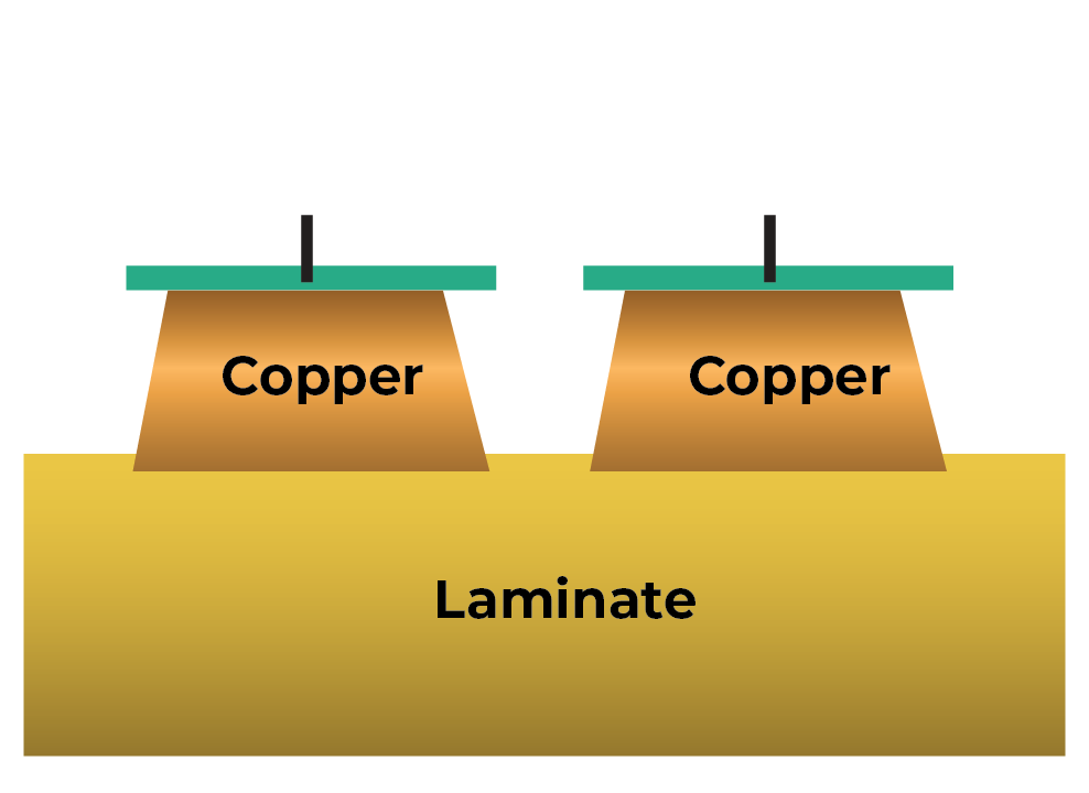
LEADING THE INDUSTRY BEYOND INCUMBENT TECHNOLOGIES

PCT’s Revolutionary Technology is redefining the future of advanced ultra high-density circuit fabrication. By leveraging advanced high-performance materials and innovative additive manufacturing processes, we achieve unparalleled miniaturization of circuit geometry and signal integrity. Moreover, our commitment to environmental sustainability ensures that our advanced fabrication techniques are not only leading the industry but also minimizing environmental impact.

Limitations of Standard PCB Manufacturing

Traditional printed circuit board (PCB) manufacturing processes, which rely on electroless copper plating to build up copper, and subtractive chemical etching to remove unwanted copper, face inherent challenges as the industry advances toward ultra high-density circuitry. These challenges include:

Limits on Miniaturization

Standard PCB fabrication technology is nearing its practical limits for reducing the size of circuit lines and spaces, struggling to meet the miniaturization needs of high-performance ultra high-density, fine-pitched circuit designs.

Subtractive etching removes material both sideways and downward, which can result in traces being etched away if the lines and spaces are too fine. Many domestic PCB suppliers can fabricate 75-micron lines and spaces with multi-layer construction. While some suppliers can produce circuits with 50-micron lines and spaces, the number of capable suppliers dramatically decreases for lines and spaces below 50 microns.

Environmental and Health Risks

Conventional wet metallization and etching processes, involve immersing the PCB in numerous chemical baths, many of which contain toxic solvents. These pose significant environment hazards and health risks to handlers.

These processes generate substantial hazardous waste, including copper-containing effluents. Without effective management and treatment, these pollutants pose serious risks to water quality and the aquatic ecosystem health.

Supply Chain Vulnerabilities

Asia has long been the preferred region for PCB fabrication due to low-cost labor, abundant natural resources, supportive government policies, and large investments in infrastructure. However, recent geopolitical events have exposed significant logistical vulnerabilities in the Asian supply chain, extending lead times and prompting many domestic electronics companies to seek alternate sources.

The CHIPS Act, a critical piece of U.S. legislation aimed at diminishing reliance on foreign manufacturers, is offering substantial grants to foster domestic research and development initiatives, and bolster manufacturing infrastructure in the United States.

The Emergence of Additive PCB Manufacturing Technology

Extensive research and development efforts have been dedicated to advancing PCB fabrication technology, with additive manufacturing emerging as a major focus. Rather than removing unwanted material through etching (as in traditional subtractive methods), this innovative approach constructs circuits sequentially by adding dielectric and conductive materials layer-by- layer.

Key Aspects

  • Layer-by-Layer Construction
  • Thinner Multi-Layer Stacks
  • Finer Lines & Spaces
  • Utilizes Advanced Polymer Substrate Materials
  • Can Include Semi-Additive Processes (SAP & mSAP)

Advantages

  • Capable of Finer & Denser Features in the 25- to 50-micron range
  • Enables Complex & Intricate Designs
  • Allows Rapid Prototyping
  • Reduces Use of Hazardous Chemicals

Challenges

  • Requires Some Specialized Equipment & Processes
  • Needs Precision Process Controls
  • Demands Expertise in Materials Science
  • Void & Lamination Defects Reduce Yields & Limit Layer Count

Precision Circuit Technology has established itself as a leader in additive PBC manufacturing, overcoming challenges and achieving precision control over feature sizes and performance. PCT has successfully produced traces as small as 6 microns, while holding tolerances to 1 micron, setting a new standard in the industry.