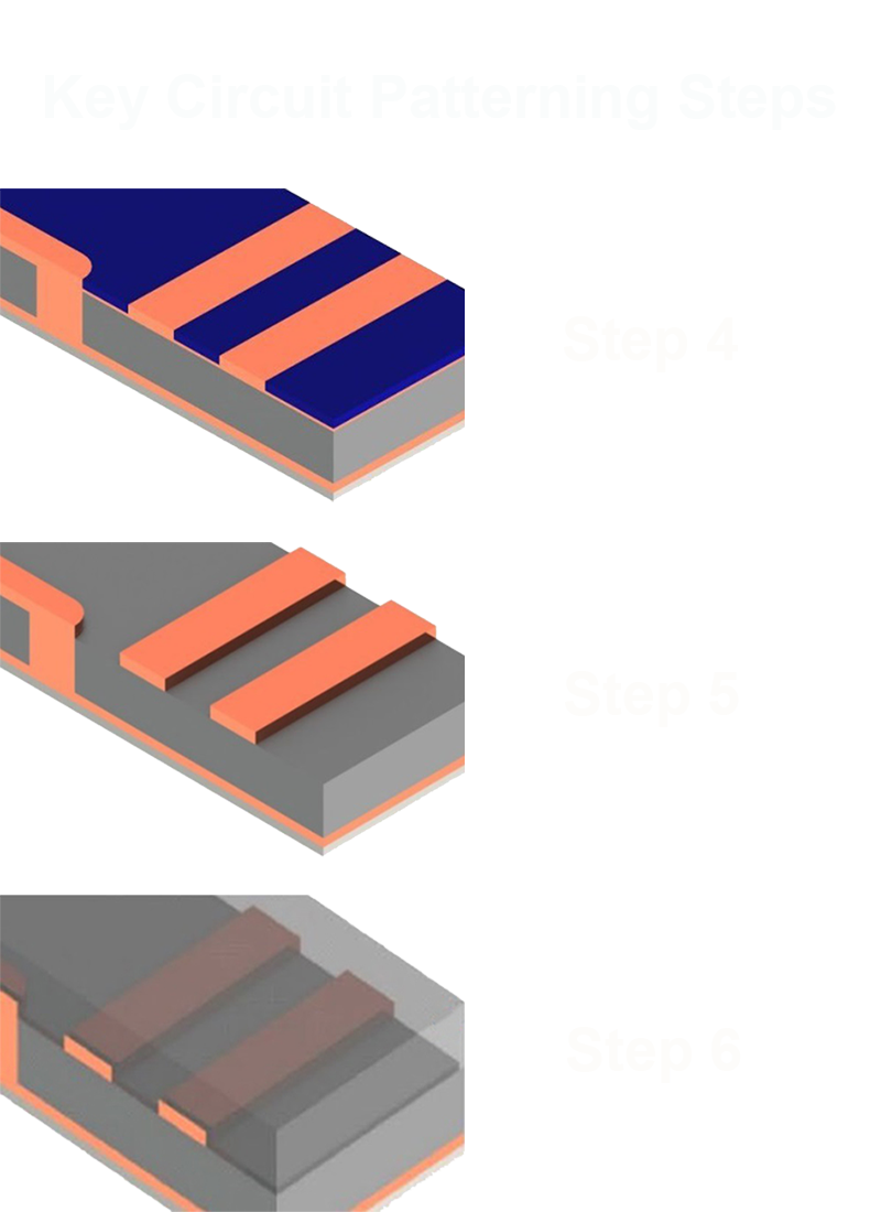
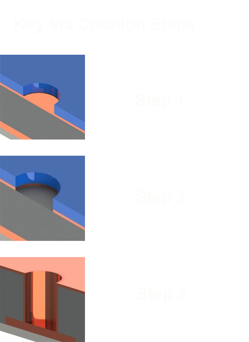
Proprietary Additive Manufacturing Processes

Precision Circuit Technology features two distinct ultra high-density circuit fabrication channels. By utilizing both semi-additive and fully additive processes, we can provide comprehensive solutions tailored to diverse needs and requirements. Leveraging these advanced fabrication techniques, we meet the demands of today’s modern electronics and are well positioned to tackle the challenges of next-generation devices.

The PCT Semi-Additive Process (SAP)

Our SAP process constructs circuit features and geometry with precision control, maintaining tolerances to 1 micron. We can adjust traces, making them wider or thinner, and even embed traces directly in the LCP substrate, moving them closer to the ground plane to achieve precise impedance matching.

SAP Resist-Defined Circuit Pattern Plating

  • Step 1 – Start with LCP copper laminate film.
  • Step 2 – Micro-etch copper from 9 microns to 3 microns. This thin field layer of copper functions as a seed layer catalyst for the deposition process.
  • Step 3 – Apply plate resist to define the circuit pattern.
  • Step 4 – Grow the circuit pattern.
    Our proprietary semi-additive technique grows circuits vertically in a process that is 90% greener than conventional plating.
  • Step 5 – Micro-etch unwanted seed layer remnants.
    Our fast micro-etch process preserves straight sidewalls on traces.
  • Step 6 – Laminate the next layer of LCP.
    We can build circuit stacks up to 30 layers or more.

SAP Via Creation: Laser Ablation

  • Step 1 – Apply clearance resist.
    Defines exact size and location of via.
  • Step 2 – Micro-etch field copper to desired diameter.
  • Step 3 – Laser ablation of LCP.
    Creates via cylinder without damaging the base copper.
  • Step 4 – Metallize side walls with precision-controlled process.
    Vias grow from the bottom up with vertical side walls.

Our via creation process is optimized for multi-layer stacks. Vias can be of the same size or of varied sizes. They are precisely aligned center-to-center, with no plating voids or side wall taper.

PCT’s Fully Additive Circuit Printing Processes

Our fully additive circuit printing process leverages specialized 3D PCB printing equipment, advanced particle-free conductive inks and ultra low-loss LCP dielectric ink to construct UHDI circuitry. These processes are ideal for rapid prototyping, low-volume production and unique circuit shapes.

Precision Dispense Platform

Dispenses higher viscosity conductive inks precisely where needed. No stencils required. Ideal for creating circuitry on rigid, rigid-flex, and flexible substrates.

25 to 50-micron lines & spaces

Precision Ink Jet Platform

With up to 8 material channels, our ink jet printing platform supports multi-material layering of low-viscosity conductive inks and ultra low-loss LCP dielectric ink.

25 to 50-mictron lines and spaces

Precision Aerosol Jet Platform

Aerosol jet printing creates ultra fine lines and spaces with 3-axis motion control, constructing multi-material circuits with unique geometries, including horizontal and diagonal vias, through-holes and embedded components.

10 to 50-mictron lines and spaces

Our state-of-the-art 3D circuit printing processes enable

✓ Diverse trace widths and heights on the same layer
✓ Varied substrate thicknesses within a single layer
✓ Unique geometries, including curves, honeycomb or cylinder-shapes
✓ Rapid prototyping, with proof-of-concept within hours, instead of days or weeks
✓ Elimination of corrosive chemical electroplating and etching processes
✓ Printing circuit stacks up to 30 layers or more
✓ Embedding die and/or passive components in the dielectric