OUR CAPABILITIES: REVOLUTIONIZING
THE FUTURE OF HIGH-DENSITY CIRCUITS

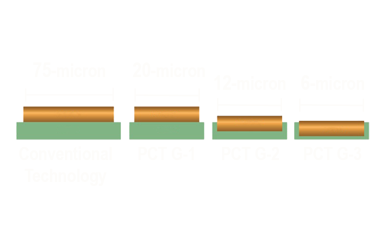
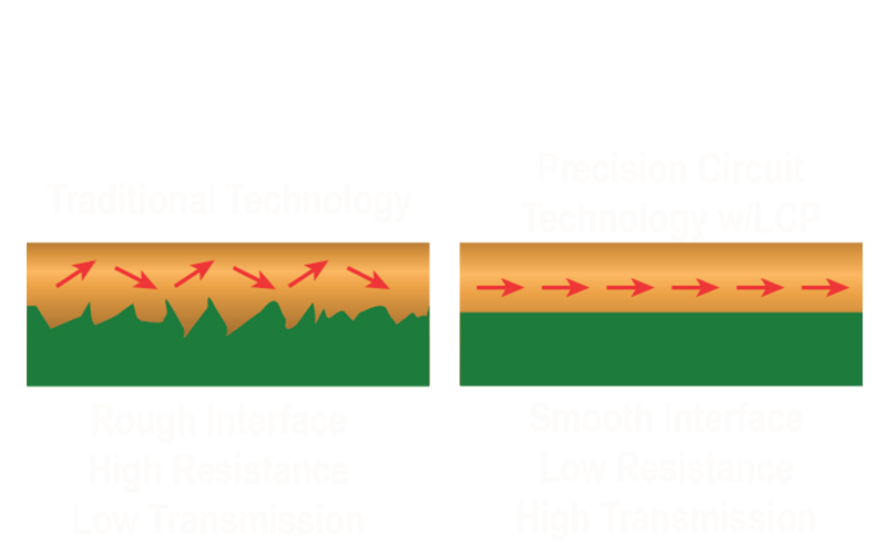
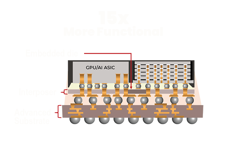
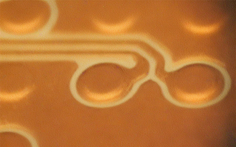
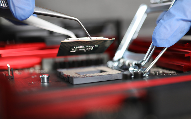
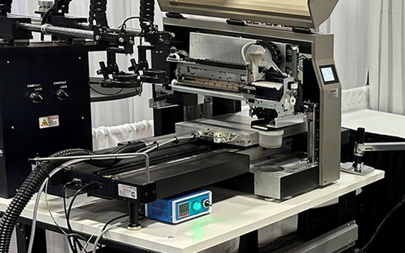
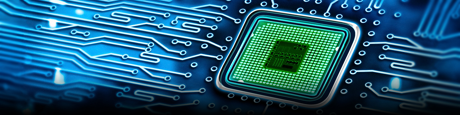
With an unwavering commitment to innovation, we are pushing the boundaries of what is possible in ultra high-density circuit design and fabrication. Our revolutionary approach not only advances UHDI circuit manufacturing but also provides engineers unprecedented design freedom and flexibility, empowering them to innovate in ways never before possible. We are privileged to share our expertise, capabilities and transformative methods, unlocking new possibilities for technological advancement.

Ultra-Thin Multi-Layer Stacks
With Liquid Crystal Polymer (LCP) 

Traditional high-performance circuit boards based on PTFE (Polytetrafluoroethylene) or glass-reinforced resins are too thick to make very small via connections between layers. Utilizing liquid crystal polymer (LCP) we build ultra-thin circuit stacks up to 30 layers.

Miniaturized Circuits 

With our proprietary liquid crystal polymer materials and additive processes, we build circuits vertically with precision-engineered straight sidewalls on traces. Our techniques achieve ultra high-density circuit geometries with lines and spaces as small as 6-microns, enabling innovative compact designs for next- generation electronics.

Superior Signal Integrity 

Our technology is ideal for high-frequency and high-data rate applications (up to 110GHz at 224 Gb/s) such as mmWave electronics, radar, filters and antenna. Using proprietary additive PCB fab techniques, advanced LCP materials and particle-free conductive inks, we craft low-loss (<0.5 dB/in) ultra high-density flexible, rigid-flex, and rigid circuits for high-RF applications.

Chip Embedding 

PCT’s capabilities extend to embedding die directly into the PCB stack and connecting chips to the circuit without the need for wires or ball grid arrays. These industry-leading die attach techniques support next-generation miniaturization and ultra high-density integrations, while offering superior electrical performance and mechanical reliability.

Precision Tolerances

Conventional processes typically maintain a 10% tolerance on a 52-micron trace, resulting in a deviation of about 5.2-microns. In contrast, PCT’s advanced fabrication techniques enables us to hold tolerances on circuit geometry to just 1-micron. This exceptional precision allows precise tuning of circuit impedance to within 1-ohm of the target value.

High-Speed Interconnects 

Our innovative pluggable sockets and connectors support up to 1000 pins in the area where current technology supports 20 to 40 pins. This advancement not only enables significantly higher I/O data rates but also simplifies functional testing and chip replacements.

Quick-Turn 3D Printed Circuits 

Current 3D circuit printing technology relies on particle-based conductive inks that require UV curing, which degrades signal integrity. PCT’s particle-free metal inks eliminate the need for curing, resulting in 3D printed circuits with excellent signal integrity.